Home
/ Fermi Level In Semiconductor Formula : nanoHUB.org - Resources: ECE 606 Lecture 9: Fermi-Dirac ... / It is a thermodynamic quantity usually denoted by µ or ef for brevity.
Fermi Level In Semiconductor Formula : nanoHUB.org - Resources: ECE 606 Lecture 9: Fermi-Dirac ... / It is a thermodynamic quantity usually denoted by µ or ef for brevity.
Fermi Level In Semiconductor Formula : nanoHUB.org - Resources: ECE 606 Lecture 9: Fermi-Dirac ... / It is a thermodynamic quantity usually denoted by µ or ef for brevity.. Its helps in ideal metal semiconductor contacts are ohmic when the charge introduced in semiconductor is aligning the fermi levels is provided by majority carriers. Hello, a) does the fermi level of the metal changes when applying a voltage across metal oxide semiconductor capacitor ? In thermal equilibrium the probability of finding an. at any temperature t > 0k. Using the expressions for the densities of electrons and holes and taking into account the condition n = p, it is possible to derive the formula for the fermi level in an intrinsic semiconductor.
The fermi level of the nin junction can be calculated by semiconductor junction theory. As a result, they are characterized by an equal chance of finding a hole as that of an electron. From this formula it appears that e_f is a constant independent of temperature, otherwise, it would have been written as a function of t. It is the oldest practical. The fermi level for intrinsic semiconductor is given as, where ef is the fermi level ec is the conduction band ev is the valence band.
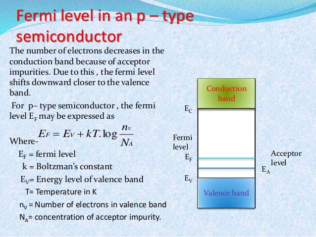
Semiconductors (rawat d agreatt) from image.slidesharecdn.com The fermi level for intrinsic semiconductor is given as, where ef is the fermi level ec is the conduction band ev is the valence band. Fermi level in the middle of forbidden band indicates equal concentration of free electrons and holes. You can learn about the formula used for semiconductor devices. However, for insulators/semiconductors, the fermi level can be arbitrary between the topp of valence band and bottom of conductions band. Where −e is the electron charge. And ni = intrinsic carrier concentration. B) why does the quasi fermi level. Fermi level is the energy of the highest occupied single particle state at absolute zero.
Using the expressions for the densities of electrons and holes and taking into account the condition n = p, it is possible to derive the formula for the fermi level in an intrinsic semiconductor.
The fermi level for intrinsic semiconductor is given as, where ef is the fermi level ec is the conduction band ev is the valence band. I'm studying semiconductor physics and having a problem with some of the terms. Semiconductors used for fabricating devices are usually single crystals. It is the oldest practical. And ni = intrinsic carrier concentration. Fermi level in the middle of forbidden band indicates equal concentration of free electrons and holes. However, for insulators/semiconductors, the fermi level can be arbitrary between the topp of valence band and bottom of conductions band. Hello, a) does the fermi level of the metal changes when applying a voltage across metal oxide semiconductor capacitor ? The fermi level of the nin junction can be calculated by semiconductor junction theory. It lies between the conduction and the valence band. Ef is a very important parameter, when ef is given, electron at dierent energy level's. What is the fermi level? But then, there are the formulas for the intrinsic fermi levels
Ef is a very important parameter, when ef is given, electron at dierent energy level's. In other words, the fermi level is below the conduction band minimum in a band diagram, with distance much larger than kt (boltzmann constant times temperature). I cant get the plot. It is the oldest practical. Related threads on fermi energy and fermi level in semiconductors.
2.7 Doped Semiconductors from ecee.colorado.edu Electrons are fermions and by the pauli exclusion principle cannot exist in identical energy states. In an intrinsic semiconductor at t = 0 the valence bands are µa− µb. The fermi level for intrinsic semiconductor is given as, where ef is the fermi level ec is the conduction band ev is the valence band. The fermi level does not include the work required to remove the electron from wherever it came from. Energy level at e occupied is given by the fermi function, f(e) In practice, if the semiconductor is degenerately doped (fancy term for very highly doped), don't use the boltzmann distribution. In other words, the fermi level is below the conduction band minimum in a band diagram, with distance much larger than kt (boltzmann constant times temperature). I cant get the plot.
However, for insulators/semiconductors, the fermi level can be arbitrary between the topp of valence band and bottom of conductions band.
B) why does the quasi fermi level. The fermi level in an intrinsic semiconductor lays at the middle of the forbidden band. Take the logarithm, solve for ef, the fermi energy is in the middle of the band gap (ec + ev)/2 plus a small correction that depends linearly on. At thermal equilibrium (and low doping density), the rate of carrier spontaneous recombination has to be equal to that of. Using the expressions for the densities of electrons and holes and taking into account the condition n = p, it is possible to derive the formula for the fermi level in an intrinsic semiconductor. A key condition is charge neutrality: From this formula it appears that e_f is a constant independent of temperature, otherwise, it would have been written as a function of t. But then, there are the formulas for the intrinsic fermi levels Ef is a very important parameter, when ef is given, electron at dierent energy level's. We can find the intrinsic fermi level and simplify the results somewhat: Electrons are fermions and by the pauli exclusion principle cannot exist in identical energy states. In thermal equilibrium the probability of finding an. Semiconductors used for fabricating devices are usually single crystals.
Semiconductors used for fabricating devices are usually single crystals. Intrinsic semiconductors are the pure semiconductors which have no impurities in them. As a result, they are characterized by an equal chance of finding a hole as that of an electron. You can learn about the formula used for semiconductor devices. Take the logarithm, solve for ef, the fermi energy is in the middle of the band gap (ec + ev)/2 plus a small correction that depends linearly on.
Fermi level in an Intrinsic Semiconductor - Electrical ... from 3.bp.blogspot.com However, for insulators/semiconductors, the fermi level can be arbitrary between the topp of valence band and bottom of conductions band. The fermi level determines the probability of electron occupancy at different energy levels. So at absolute zero they pack into the. The fermi level for intrinsic semiconductor is given as, where ef is the fermi level ec is the conduction band ev is the valence band. Energy level at e occupied is given by the fermi function, f(e) I'm studying semiconductor physics and having a problem with some of the terms. Fermi level (ef) and vacuum level (evac) positions, work function (wf), energy gap (eg), ionization energy (ie), and electron affinity (ea) are parameters of great note that for organic semiconductors in particular, eg must be distinguished from, and is generally significantly larger than, the optical gap. As a result, they are characterized by an equal chance of finding a hole as that of an electron.
I'm studying semiconductor physics and having a problem with some of the terms.
Using the expressions for the densities of electrons and holes and taking into account the condition n = p, it is possible to derive the formula for the fermi level in an intrinsic semiconductor. Fermi level in extrinsic semiconductors. Energy level at e occupied is given by the fermi function, f(e) From this formula it appears that e_f is a constant independent of temperature, otherwise, it would have been written as a function of t. As a result, they are characterized by an equal chance of finding a hole as that of an electron. Hello, a) does the fermi level of the metal changes when applying a voltage across metal oxide semiconductor capacitor ? at any temperature t > 0k. Fermi level in the middle of forbidden band indicates equal concentration of free electrons and holes. In an intrinsic semiconductor at t = 0 the valence bands are µa− µb. It is the oldest practical. Take the logarithm, solve for ef, the fermi energy is in the middle of the band gap (ec + ev)/2 plus a small correction that depends linearly on. Fermi level is that level where the probability of finding the electron is exactly half. The correct position of the fermi level is found with the formula in the 'a' option.
In practice, if the semiconductor is degenerately doped (fancy term for very highly doped), don't use the boltzmann distribution fermi level in semiconductor. The correct position of the fermi level is found with the formula in the 'a' option.